


Introduction
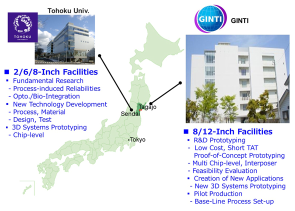
The Global INTegration Initiative (GINTI) is a 8/12-inch R&D fab for the research and development of new 2.5D/3D integration technologies and creative applications. GINTI offers a broad range of services to our customers to meet the mounting R&D needs of the semiconductor industry and related industries. We collaborate with chipmakers, equipment and materials suppliers, universities, and companies working in emerging technologies, to test new designs, integration methodologies, and prototype systems in a manufacturing environment, leveraging the experience, facilities and tools already in place in the fab. Our model provides a cost-competitive process development infrastructure in a manufacturing-like fab environment and a low-cost, short TAT prototyping of proof of concepts using commercial/customized 2D chips, and a base-line process set-up for the pilot production of creative 3D systems. GINTI aims to provide Tohoku University's advanced 3D integration technologies into electronics industries to accelerate the commercialization of innovative 3D technologies and applications into real, manufacturing-ready technology solutions with FAST.
GINTI's R&D fab is located at Miyagi's reconstruction park in Tagajo-shi nearly 15km eastside to Sendai-shi, Miyagi and provides 1500m2 of cleanroom space for the R&D and the pilot production service of new 2.5D/3D integration technologies and creative applications.
PRESS
- Global INTegration Initiative (GINTI) opening celemony has been held in Sendai, Japan. (20 Sept. 2013)
- Global INTegration Initiative (GINTI) website has been opened. (19 Sept. 2013)